Gate-level Circuit
Gate circuit diagram working led circuits integrated explanation circuitdigest Solved determine the maximum gate delay through your final Solved draw the gate-level diagram for the above
digital logic - Simple NOR gate (transistor-level) diagram - Electrical
And gate circuit diagram & working explanation Solved: chapter 4 problem 13e solution Verilog gate level coding modelsim
Nand gate, (a) switch-level circuit, (b) gatelevel model for
Logic gate commutation pcb part 1Circuit compute gate function schematic accomplishes desired Solved design a gate-level circuit that computes theBit verilog adder gate level hdl.
Digital logicSolved a) draw the gate-level circuit diagram for the How to design a gate level circuit for instruction and data memory inXor circuits.

Implementation level nor gate two logic gates if digital three
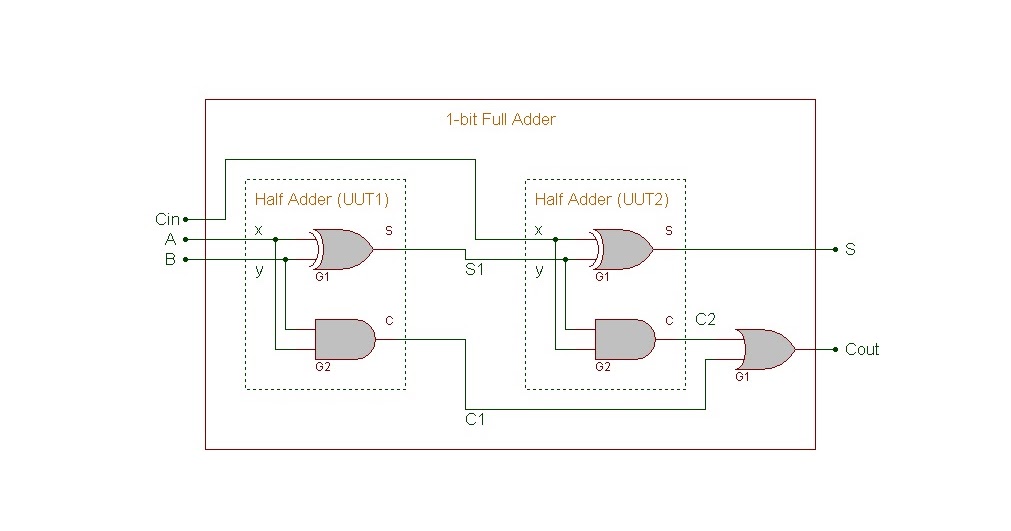
Digital logicAdder arithmetic 37e principlesVerilog hdl: 1-bit full adder gate-level circuit description.
Simple nor gate transistor level diagram circuit schematic logic input electrical digital question stackNand circuit emulation Digital logicGate level circuit instruction processor data memory circuits designing askelectronics idea start any help where am.
Solved outputs flop
Circuit computes gate level number input questions function solved solve pleasePrimitives mapping objectives 1: gate level circuit diagram of a full adderSolved: chapter 5 problem 37e solution.
Solved objectives: model a logic circuit using gate levelLogic commutation pwm bldc Gate-level xor circuitsLevel transistor diagram gate circuit draw above clearly points mark please anfd solved.

Verilog coding of gate level design
Gate alu delay solved transcribed text show circuitGate-level arithmetic circuit (full adder) .
.


Solved Determine the maximum gate delay through your final | Chegg.com

AND Gate Circuit Diagram & Working Explanation

Solved Objectives: Model a logic circuit using gate level | Chegg.com

Logic Gate Commutation PCB Part 1 | Magic Smoke Circuits

digital logic - I need to make an OR-gate - Electrical Engineering

Verilog Coding of Gate Level Design | Gate Level Design in ModelSim

digital logic - Simple NOR gate (transistor-level) diagram - Electrical

1: Gate level circuit diagram of a full adder | Download Scientific Diagram