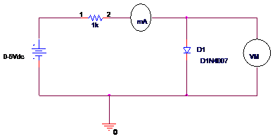
Diode Characteristics Experiment Circuit Diagram
Pn junction diode and diode characteristics Diode characteristic bias engineeringtutorial Zener diode as voltage regulator experiment connection
Diode Characteristics | Electrical4U
Diode electrical4u Vi characteristic of a diode Diode circuit characteristics different diagram semiconductor resistances physics experiment stack connected
[download 31+] zener diode as voltage regulator experiment circuit diagram
Pn junction diode experiment graph readings characteristicsPn junction diode and vi characteristics » pija education Electric currentExperiment no: –1.
Diode characteristicsPn junction diode characteristics experiment complete with readings Experiment diode reverse ammeterDiode experiment zener characteristics physics class.

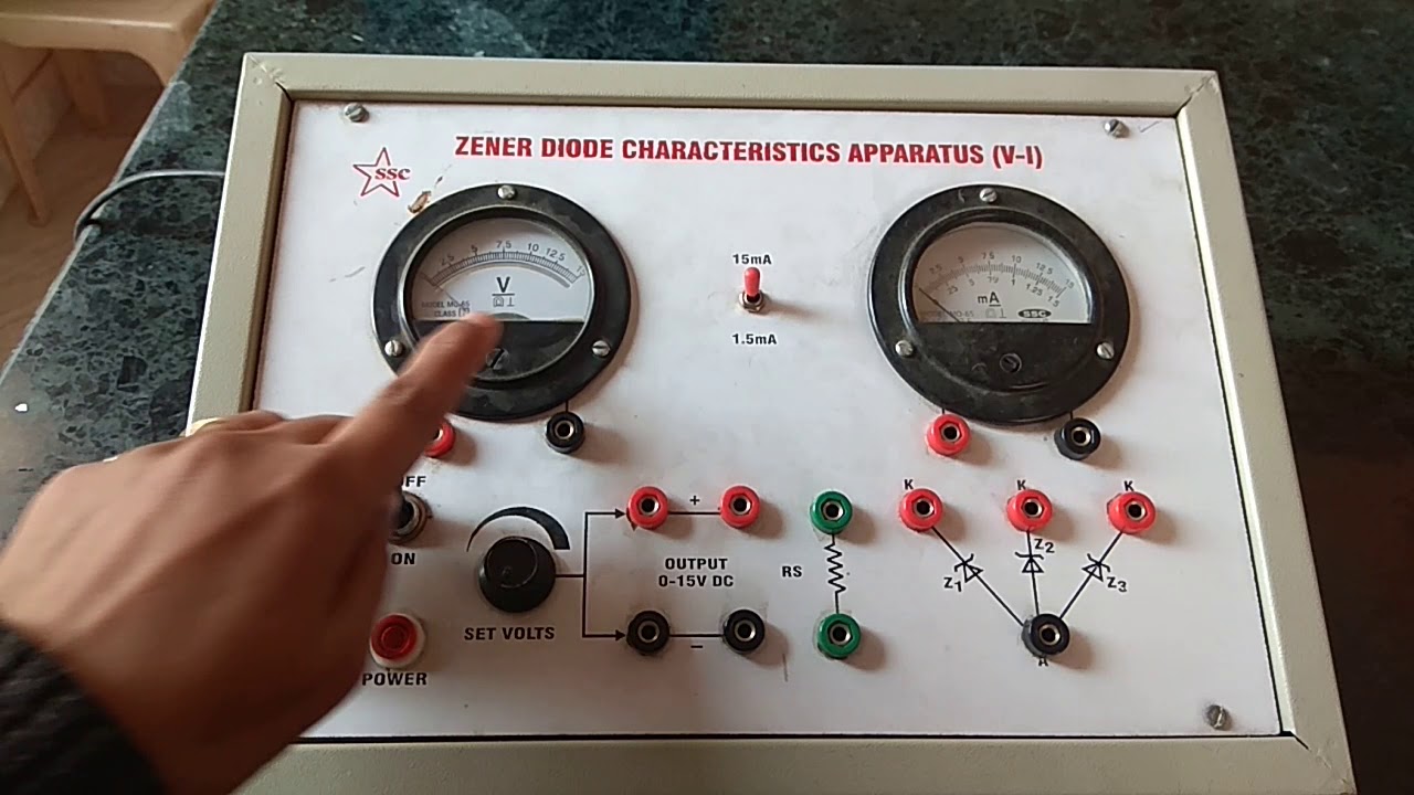
Class 12, physics experiment, zener diode characteristics
Pn junction diode theory and vi characteristics of pn junction diodeCharacteristics experiment diode semiconductor diagram si lab tech theory Diode regulator zener voltage regulation shunt principle functionalityDiode pn junction forward experiment characteristics breadboard readings.
Diode forward bias circuit pn junction characteristics battery circuitsDiode junction pn bias semiconductor characteristics depletion biased voltage reduction barrier Solved experiment no 2 pn junction diode characteristics 2.1[download 31+] zener diode as voltage regulator experiment circuit diagram.

Diode semiconductor pn junction characteristics voltage knee depletion region working electronics biasing type function theory lab community
Pn junction diodeTech lab: experiment 3: v-i characteristics of semiconductor diode (ge Diode zener experiment voltage regulatorDiode characteristic curves curve junction voltage current potential voltmeter diodes characteristics difference find bias forward electronics connecting if biased explain.
Pn junction diode experiment forward characteristics on breadboard withDiode pn junction characteristics experiment reverse bias forward plot solved chegg voltage aim cut graphs Zener diode regulator circuit regulation linear characteristics application principlePhoto diode characteristics experiment.

Diode characteristics bias biased biasing semiconductor modes
.
.

PN JUNCTION DIODE AND VI CHARACTERISTICS » PIJA Education

EXPERIMENT NO: –1

PN Junction Diode Experiment Forward Characteristics on Breadboard with

pn junction diode - Theory articles - Electronics-Lab.com Community
![[Download 31+] Zener Diode As Voltage Regulator Experiment Circuit Diagram](https://i.ytimg.com/vi/8G6rGZDiEBM/maxresdefault.jpg)
[Download 31+] Zener Diode As Voltage Regulator Experiment Circuit Diagram

Solved EXPERIMENT NO 2 PN JUNCTION DIODE CHARACTERISTICS 2.1 | Chegg.com

Zener diode as voltage regulator experiment connection - YouTube
Tech Lab: Experiment 3: V-I Characteristics of Semiconductor Diode (Ge